8-Bit Digital Computer-(01)
Monostable and Bistable modes in clock module
We have discussed the astable mode in the previous blog. Now let’s discuss the remaining two modes.
The Manual Mode-Monostable
There are times when you want to catch a clock signal and debug it. Let’s explore a few possibilities.
Basic circuitary:
This situation can be handled by a simple circuit using a push button. But whenever we switch from any state, there is some contact bounce, which leads to makes and breaks for a few milliseconds before settling in the closed position. The issue here is the bouncing of the push button. The circuit is shown below:


We might all have gone through this bouncing issue during the flickering of the tube light.
Resolving:
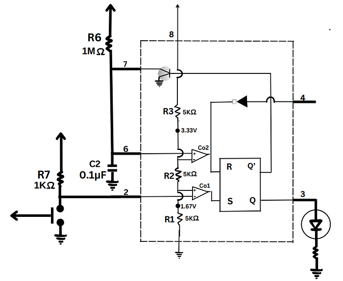
To resolve this issue, we should have an exact state change, which can be done by accessing the SR latch (discussed in the previous blog) in the 555 IC Timer and using it in between the pins, as shown below.


The timing diagram explains the debouncing behavior of the circuit that we have shown above. On pressing the pins, we see that the bouncing part in pin 1 and pin 2 is not there in the Q and Q’.
Debouncing occurs when pressing the push button multiple times; it gives a single output signal, and the bouncing of the push button does not affect the signal.
But this alone is not enough. We are not just using this to change states; we also want to produce a pulse signal, so we are using an RC circuit to control the time period, which is the pulse width of the signal.
Building the debouncing circuit:
On pressing the push button,it triggers the negative terminal of the comparator Co1, which was initially connected to a resistor, giving the voltage drop. It should not be below 1.67 volts, so a resistor of 1 kiloohm is connected.
And the RC circuit is separately connected at pin 6 and pin 7. The resistor and capacitor decide how long the LED should glow, which is the time period of the pulse. We select the value accordingly. We want the led to be on for a reasonable amount of time, so a capacitor of 0.1 microfarad and a resistor of 1 megaohm are connected. We already discussed the time period in the previous blog.
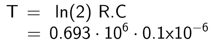
The time period comes out to be 0.0693 seconds.
And pins 6 and 7 are short-circuited as there is no more voltage drop required, and the voltage should go above 3.33 volts for the comparator to turn on.
The LED is connected at pin 3 with a 220 ohm resistor. And the pin diagram for this is shown below:
Working:
On pressing the push button, we are giving zero volts at the negative terminal of comparator 1. The set goes high, and the LED turns on, which, on the other hand, is a capacitor charging as there is current flowing through the RC circuit. On relaxing the push button, the LED goes off as the voltage at the negative terminal of the comparator goes high and the voltage is more than 1.67 volts at the negative terminal, which in turn resets the latch that triggers the base current,and it leads to the flow of current through the transistor acting as a sink. The capacitor starts discharging as there is no current flow across the RC circuit, and the voltage drops. And the latch stays in the reset state until triggered by the push button.
On continued pressing of the push button, the capacitor stays in the charged state and discharges on relaxing the button.
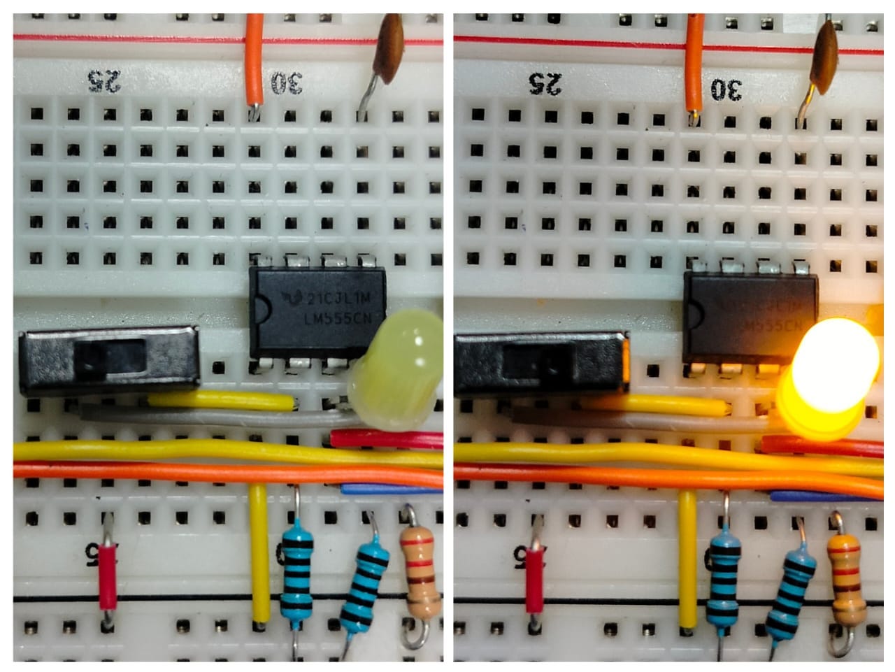
In the RC circuit, the LED is on during the charging of the capacitor, which is controlled by the push button. It is shown clearly in the oscilloscope graph output of the circuit across the LED, which is shown in yellow, and across the capacitor in blue.

We have successfully built the monostable debouncing circuit. Now let's get to the next mode, which helps us shift between these two modes.
The selecting mode-Bistable
In order to select between the monostable and astable modes, we use this bistable mode as the selecting mode. In this mode, it is stable in both states, whether it is on or off.
Same strategy:
In this way, we can also connect a switch directly and select between two modes.But there is the same issue of the switch bouncing. So we are using the same strategy by connecting the SR latch in the 555 IC timer in between the switch pins to build the debouncing circuit, as shown above in the resolving part.
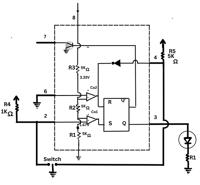
But now it is just an on-or-off switch. We are not worried about the pulse width, time period of the signal, or whether we stay in the other state for a short period of time and come back to the stable state, so we are going to directly use the latching operation of the SR latch by connecting the switch in between the pin 4 Reset button and pin 2 in the 555 IC Timer.
Assembling the selecting mode:
The 555 IC timer helps in debouncing the output. We are using a two-way switch, in which the first one or second one are connected to pins 2 and 4, respectively, in the 555 IC Timer.And when switching the pins, it gets grounded accordingly.
The switch is connected across trigger pin 2 and the output pin 4. We are using reset pin 4, which ultimately will give the reverse of the input value because of the invertor in pin 4 and the resistor of 1 megaohm connected at pin 4 across the 5 volts to maintain the constant voltage, and the invertor inverts it and maintains the off state. Pin 6 is grounded. Similarly, when the low supply is given at pin 4, the invertor will convert it, giving a high output and resetting the latch. Hence,the second pin of the switch is connected to pin 4 for direct resetting of the S-R latch.
The LED is connected at pin 3 with a 220 ohm resistor. The circuit will look as follows:
How does it work?
On switching the switch, one time it will connect the first pin to ground, and on switching the switch next time, it will connect the second one to ground. Just say on swithcing one time,it will connect the second pin to ground. There will be 1.67 volts at the positive terminal of the comparator Co1, which will set the latch and give output. Similarly, on the next switch, it will connect pin 4 to ground. So, pin 4 will take low input, which in turn will give high, reset the latch, and the LED goes off and the second pin is on.
Till now, we have only seen the debouncing of the switch.Let's say the first pin corresponds to the astable mode and the second one to the monostable mode. Now we will see how we integrate all this together.
Completion of the clock module:
Now we are going to connect all three modes together in order to complete the clock module. For this, we are going to use some AND and OR logic gates, which help in making decisions. The way to connect the signal of the three modes with the logic gate is...
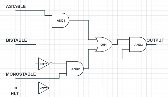
We want bistable to select between astable and monostable mode; if it selects one, the other should go off, so we are using a NOT gate. Not just this, the bistable mode should also be on at that point; only then should it pass, so we are connected through the AND gate, and these gates are connected through the OR gate because any one of them goes on, and the LED should go on. And finally, there might be situations where we need to completely turn off the computer. At those times, we give the Halt condition, which means it will go high, so we are connecting a NOT gate with an AND gate and the prior OR gate such that it gives output only if both are on.
Here, the connections can be seen from the image attached above. The clock module is done now. When the Bistable mode is off, at that time it will work with the monostable mode, and when the Bistable mode is on, it will work with the Astable mode.
The workings of the clock module are attached at the below link:
